How to Design a PCB Layout: A Comprehensive Guide
Par un écrivain mystérieux
Last updated 07 juillet 2024
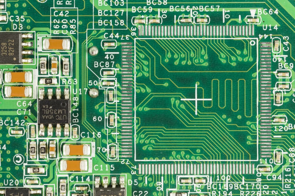
Printed Circuit Boards (PCBs) are an essential component of nearly every electronic device, providing the foundation for the connections and features that enable functionality. As technology advances and devices become more complex, the importance of efficient and effective PCB layout design has become increasingly critical. This article will guide you through designing a PCB layout, from understanding the basics to mastering advanced techniques and preparing for manufacturing.

Printed circuit board - Wikipedia
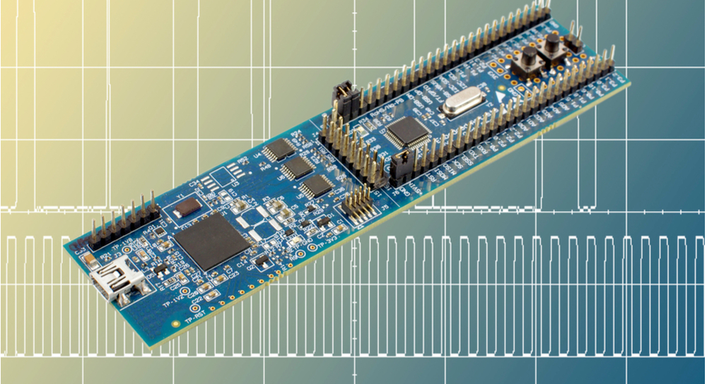
6 Layer PCB Design and Manufacturing
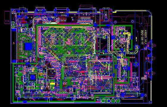
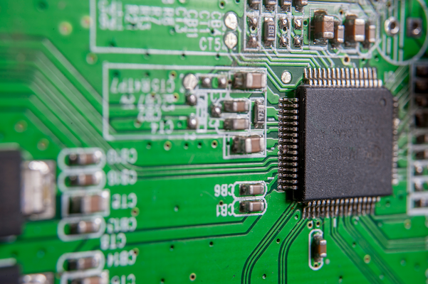
Ultimate Guide to PCB Layout Design Considerations
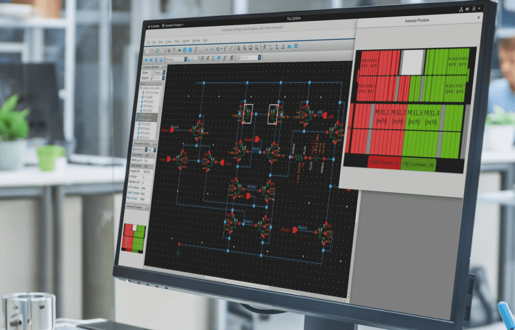
PCB Layout Simulation: A Comprehensive Guide to Designing and

PCB Testing: PCB Testing: A Comprehensive Guide to Techniques
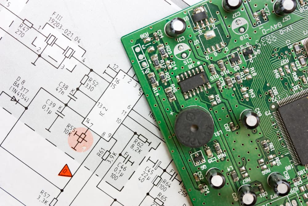
Understanding Circuit Boards - Ultra Librarian
Strategies on Designing PCB Layout - MOKO Technology
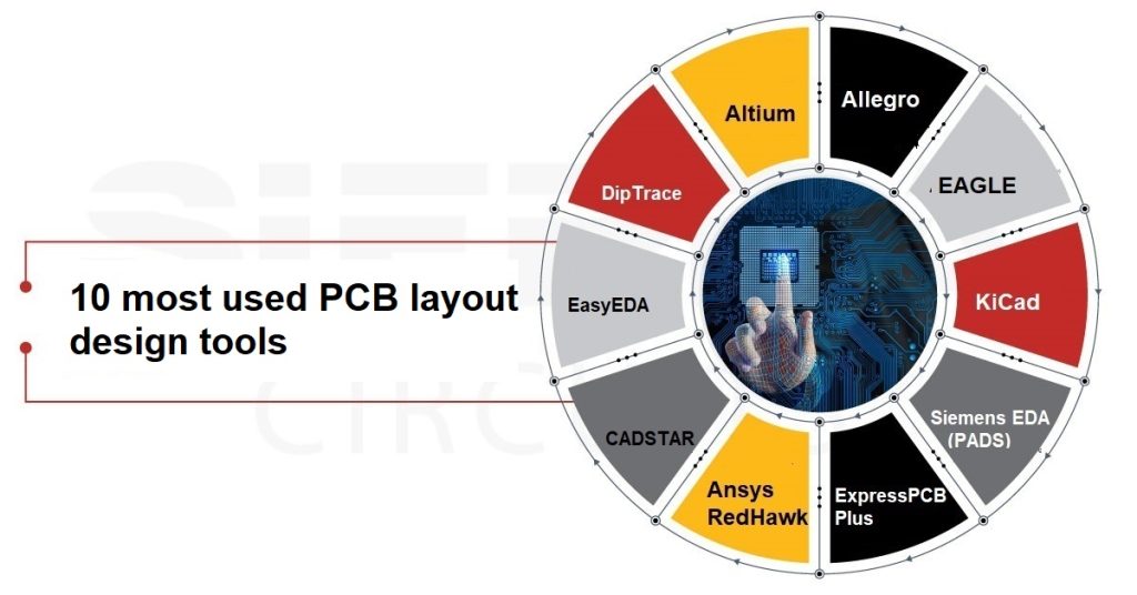
10 Most Used PCB Layout Design Tools

Simulating Designing of Circuits+PCB on Proteus : 10 Steps
Intro to PCB Design: How to Design a Circuit Board in 10 Easy Steps

KiCAD 7 PCB Layout in 5 steps

About us
Recommandé pour vous
 The Basics of A Printed Circuit Board: How Does a Circuit Board Work?14 Jul 2023
 PCB design - from idea to dedicated prototype14 Jul 2023
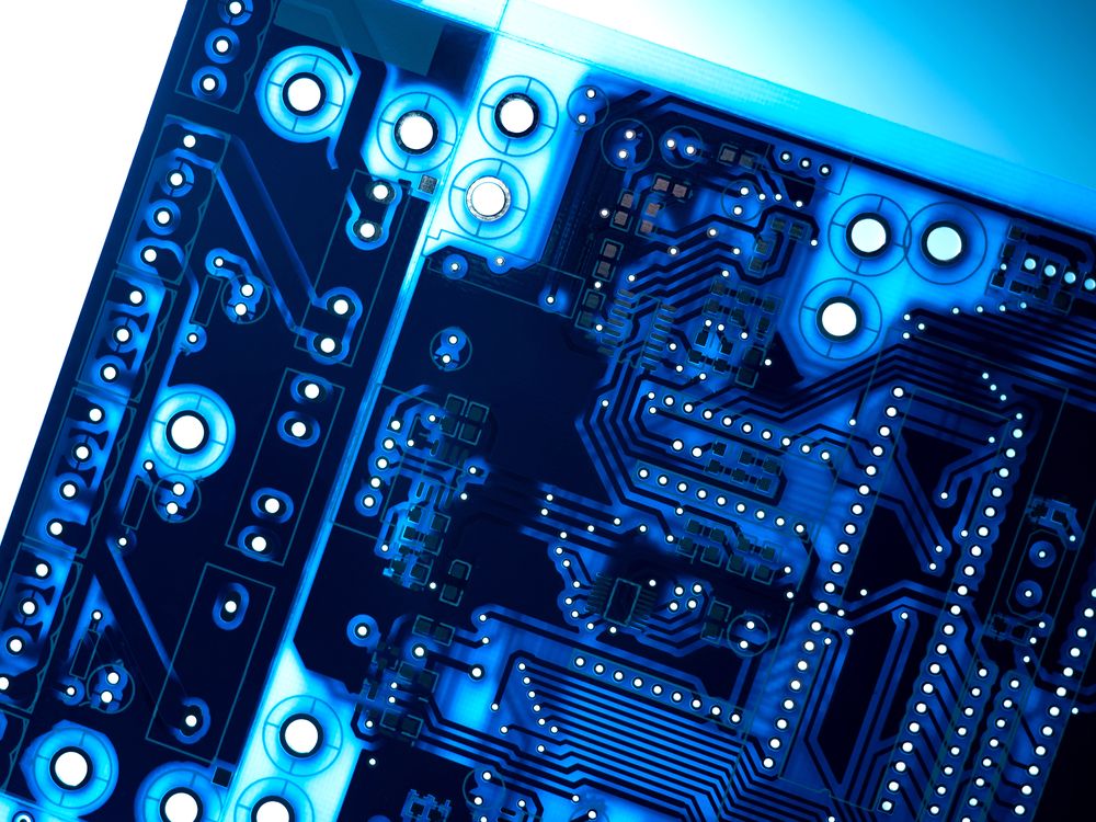 All About PCB Tooling Holes: What They Are and Where They Go14 Jul 2023
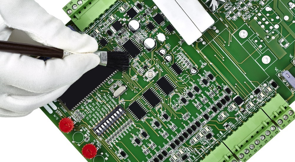 Cleaning Circuit Boards: A Comprehensive Guide14 Jul 2023
 The 2022 List of Top 10 Printed Circuit Board Manufacturers14 Jul 2023
 PCB vs IC - what are the differences - IBE Electronics14 Jul 2023
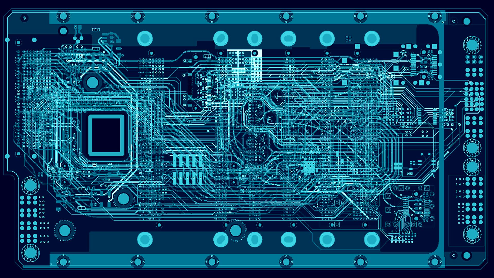 Electronic systems design and manufacturing14 Jul 2023
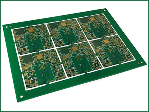 PCB (Printed Circuit Board) Panel Design Consideration14 Jul 2023
 PCB Capacitors Unveiled: Types, Uses, and Selection - MorePCB14 Jul 2023
 PCB Concepts and Materials : 4 Steps - Instructables14 Jul 2023
Tu pourrais aussi aimer
 TIMIO is the ultimate screen-free teaching toy for babies, toddlers, and young kids14 Jul 2023
 Sac shopping pliable - pas-à-pas avec photos14 Jul 2023
 Pochette kidizoom vtech - VTech | Beebs14 Jul 2023
 Clips et attache-cables murales Clips Cable Organisateur Bureau,Lot de 3 Support de Cable,Organisateur14 Jul 2023
 AK® Ruban de masquage 10 mm 18 mètres AK918514 Jul 2023
 Chauffeuse - matelas d'appoint pliant - fauteuil convertible - inclinaison dossier réglable 5 positions - tissu polyester aspect lin gris - Fauteuil de relaxation - Achat & prix14 Jul 2023
 Jouet en Bois Boite a Outil Enfant Montessori Educatif Jouet Bricolage Jeux de Construction Caisse a Outils pour Garçons Filles 3 4 5 6+ Ans, 29 Pièces14 Jul 2023
 Taie d'oreiller lin lavé bleu cobalt 65x65 cm14 Jul 2023
 MTG reveals Doctor Who Commander decks & release date - Dexerto14 Jul 2023
- Swim Essentials Piscine gonflable enfant design zèbre 150 cm14 Jul 2023